Radiated Emission failure analysis at Vougavent

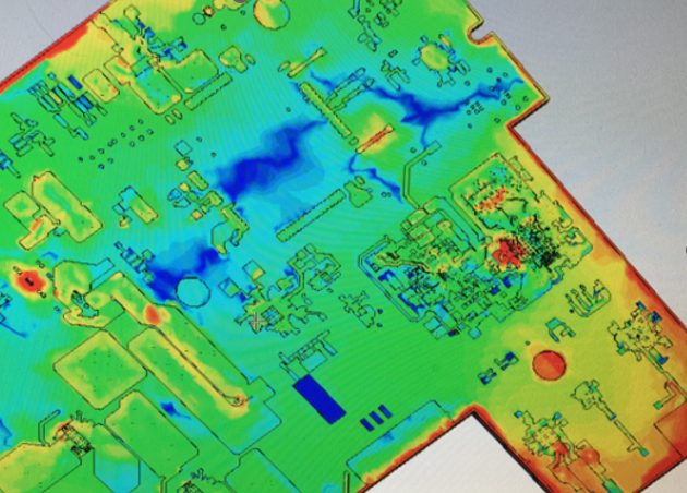
Simulation of EMC behavior
EMI (Electromagnetic Interference) and EMC (Electromagnetic
Compatibility) are critical considerations in the design and
development of electronic devices and systems. EMI and EMC
compliance is essential for ensuring that electronic devices and
systems operate correctly and do not interfere with other electronic
devices.
At Vougavent, we specialize in EMI-EMC consulting services for a wide
range of electronic devices and systems. Our team of experts has
extensive experience in the design and development of electronic
devices and systems, and can help ensure that your products meet EMI
and EMC compliance requirements.
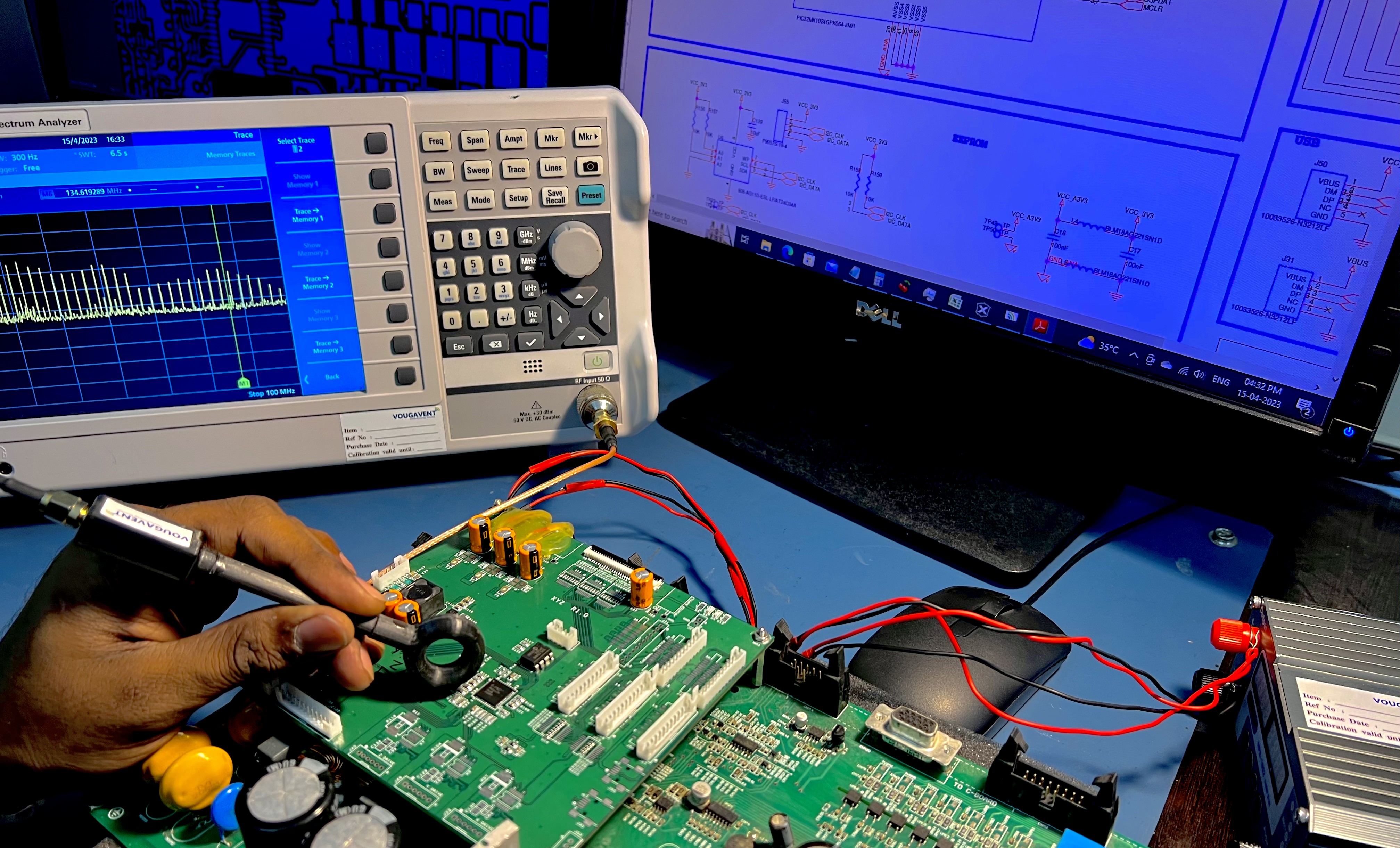
Located at Bangalore, India Vougavent has a measurement facility for debugging and analysing the EMI-EMC Performance. Our inhouse facility, support the following Measurements.


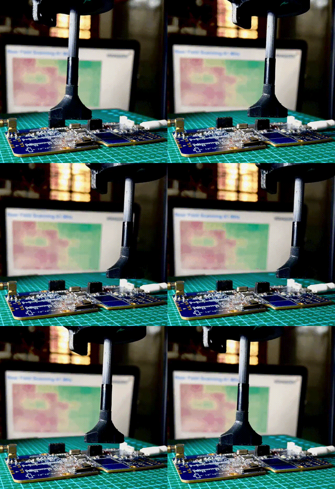
We provide the EMI nearfield scanning service to support Emission analysis. Near field scanning enable quick identification of noise sources and hot spots in the PCB. By using the EMI Near field probing faster turn around is possible for EMI failure analysis at Vougavent
| Domain | Specifications |
|---|---|
| Defense | MIL-STD 461 E,F,G |
| Aeronautical | DO-160 |
| Automotive | CISPR-25 ECE-R10 AIS-004 |
| Industrial, Scientific and Medical | CISPR-22 CISPR-11 CISPR-32 |
| CE and FCC | FCC 47 CFR Part 15 |
| IEC and EN Standards | EN 55011, IEC 61000-6-4, IEC 61000-4-4 |
Ans: Our typical lead time is 10 Working days, it depends on the complexity of the product and failure
Ans: All projects will initiated with Mutual NDAs and We adhere strictly to the Vougavent Data Protection guidelines which ensures proper handling of customer data and disposal of the data after the completion of project. For details refer Vougavent Data protection Policy Link: Vougavent Data protection policy
Ans: We have facility for RF Emission, RF Susceptibility/Immunity and Electrostatic Discharge (ESD)
Ans: We required following information, Product overview, Schematics(searchable pdf file), BOM, PCB Layout(*.pcb or *.brd with odb++) and Mechanical design (*.stp)